Nanostructures and applied spectroscopy Research Group
Department
Applied and Nonlinear Optics Research
Group leader: Veres Miklós
Webpage: https://www.szfki.hu/en/nanostr
Publications of the group: link to the database of the Hungarian Scientific Bibliography
This group has rich experiences in the field of preparation and investigation of amorphous thin films. The investigations have been focused to look for connections between structure and such macroscopical properties, like electrical transport, optical properties, photo-conductivity and photoluminescence. Most of the equipment, which are needed to the preparation and investigation of the samples are operated by the group. In the last few years the group have been dealing with hydrogenated amorphous carbon (a-C:H) films, and mostly with those, showing diamond-like properties. These films are prepared by radio-frequency (rf) glow discharge from different organic materials (methane, benzene and others) by controlling the preparation conditions, like the gas composition, flow rate, gas pressure, and rf power. The physical properties of the films prepared in this way can be varied in a broad range.
Photoluminescence (PL) investigations of a-C:H thin layers prepared either from methane or benzene source gases were performed with aim to specify the whole range of light emitted by these samples what contributes considerably to a further understanding of the fine structure of the electron density of states and the details of the radiative recombination in this material. We have shown composite feature of PL spectra, consisting of numerou characteristic bands, some of these appear already in the visible range of excitation, the others can be excited by UV light only. Three peaks with maximum position in the range of 4.34 - 4.50 eV, 3.93 - 4.01 eV and 3.64 - 3.70 eV are in the ultraviolet region. Additional peaks appear in the region of 3.17-3.22 eV and 2.85 - 2.92 eV beside the well-known broad PL band with maximum in the 2.1 - 2.33 eV range. The relative intensity of new bands vary on deposition conditions. Our results measured on numerous samples strongly suggest the existence of some type of intrinsic radiative centers.
The growth process of the carbon film was followed by IR spectra, by investigating film prepared under different deposition conditions. Surprisingly good spectral resolution could be achieved on samples deposited from benzene as source gas at relatively high pressure and low voltage conditions. Because the C-H bond-stretching region contains intensive aromatic components, we draw the conclusion, that the benzene ring structure can survive the deposition condition in the plasma, the ionization could eliminate hydrogen atom from the molecule. The structure will probably have a high active surface, what might have practical application possibilities.
New Raman spectrometer was installed this year in our group. The access to two different laser excitation makes dispersion measurements also possible.
Optical strength of a-C:H thin layers was investigated under influence of UV laser pulses in the ns and fs region on different laser wavelength. The possible utilization of these films in laser and microelectronic technology motivates these studies. The damaged area was found to depend linearly on the laser fluence in a narrow region around the damage threshold tested by rising number of pulses and fluence. The 2 - 3 times higher optical damage strength for fs pulses on both wavelengths used, can be explained by the different weights of electronic and thermal processes in the case of strongly different pulse lengths. Accumulative effects for multiple pulse impact were detected which was more clearly developed for UV region. The incubation process was the shortest for the long pulse length.
Further information:
Miklós Veres, E-mail: veres.miklos@wigner.tma.hu

Latest results
Color centers in nanodiamond. — Among the numerous optically active defects (color centers), studied in nanosized diamond (ND), the silicon-vacancy (SiV) center is a promising candidate for utilization in different fields like quantum computing and cryptography, nanoscopy, medicine or cell biology. Most applications are based on the intensive and narrow zero-phonon emission line (ZPL) of the mentioned color center, which can be detected in near infrared wavelength region, around 1.68 eV (738 nm). However, the asymmetric lineshape of the SiV ZPL may restrict the spectral parameters important for different applications and prohibit the determination of the real ZPL characteristics by traditional spectroscopic techniques.
Micro-photoluminescence measurements performed on a high number of CVD nanodiamond films containing SiV centers showed that the undesirable asymmetric tail on the low-energy side of the ZPL is related to another optically active defect (so called GR1 center) being present in the nanodiamond structures as well. Regions with relatively high GR1 content and with well-distinguishable zero-phonon lines related to different optically active defect structures can be localized by mapping of the ND film with an appropriate excitation wavelength (Fig. 1).
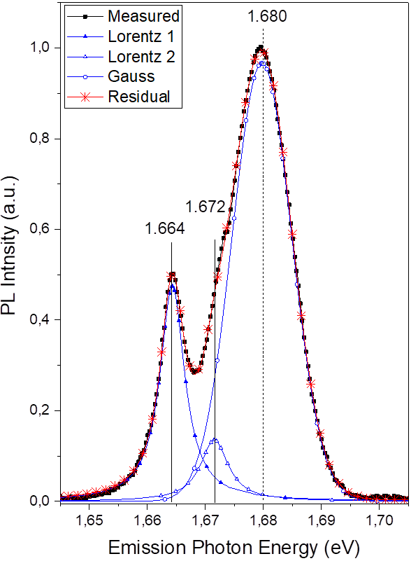
Figure 1. Fine-structured emission spectrum of CVD nanodiamond film around the SiV center ZPL region excited by 635 nm and recorded at room temperature. The deconvoluted peaks correspond to SiV center ZPL (1.680 eV) and the double ZPL of the GR1 defect (1.664 eV and the weak shoulder at 1.672 eV).
Preparation of new tetragonal silicon polymorphs by ultrashort laser pulses. — Tetragonal polymorphs of silicon were created successfully by irradiation of microcrystalline silicon powder with femtosecond laser pulses (800 nm center wavelength with 1 kHz repetition rate and 42 fs pulse duration) in air at room temperature. Surface enhanced Raman spectroscopy and, in collaboration with the Research Institute for Materials Science, Centre for Energy Research, HAS and the Research Centre for Natural Sciences, HAS, transmission electron microscopy (TEM) measurements were carried out to prove the presence of bt8 (Fig. 2) and t32* (Fig. 3) Si phases.
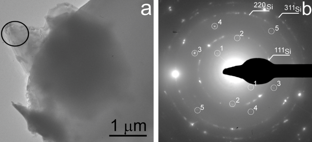
Figure 2. TEM image of bt8 Si polymorph. In addition to ordinary cubic Si, weak extra reflections occur with the following d spacings: 4.70 (1), 3.37 (2), 2.60 (3), 2.38 (4), 2.10 (5) Å. These extra reflections are consistent with {101} (1), {200} (2), {211} (3), {220} (4) and {301} (5) reflections of bt8 Si.
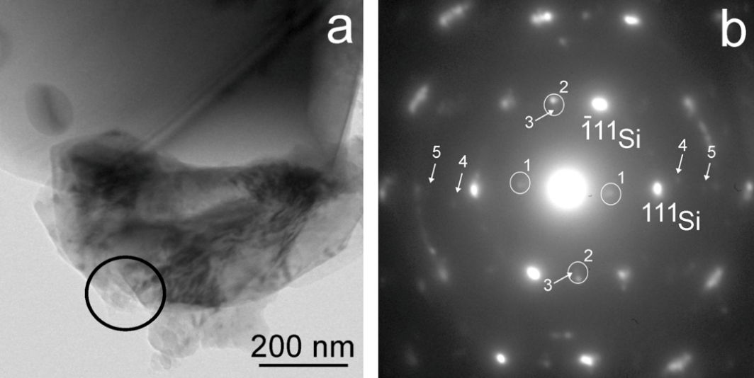
Figure 3. TEM image of t32* Si polymorph. In addition to ordinary cubic Si, there are two sets of strong reflections with 6.60 (1) and 3.20 (2) Å. These strong reflections and their measured angles are consistent with {110} and {0-12} of t32* Si grain. The additional weak reflections with 3.63 (3), 2.65 (4), 2.16 (5) Å can be interpreted with {211}, {311} and {013} of t32* Si.
Results in 2016
Silicon-vacancy center in nanodiamonds. – Due to their excellent light emission properties, the investigation of the negatively charged silicon–vacancy (SiV−) centers in diamond nanostructures has attracted much interest during last decades. The SiV− center consisting of one interstitial silicon atom in a split–vacancy configuration with D3d symmetry has a bright, stable and narrow zero-phonon line (ZPL) at 1.681 eV. It has a weak phonon sideband since more than 70% of the emitted light is concentrated into the ZPL even at room temperature. These advantageous properties of the optical transition make the SiV– center a promising candidate for solid-state single-photon emitter that can be used to realize numerous novel applications in quantum computing and cryptography or nanoscopy and cell biology, etc. For quantum information and quantum processing purposes, indistinguishable single photons from distinct SiV− center emitters are required. Variation of spectral parameters of the mentioned center observed by different groups strongly restricts its implementation to real applications. Novel methods have to be developed for the creation of uniformly emitting silicon–vacancy centers in diamond nanostructures on large scale, and the origin of the processes responsible for the variation of the ZPL of the SiV– centers has to be resolved.
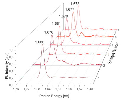
Figure 1. Spectral distribution of SiV– center emission line in photoluminescence spectra measured at room temperature in nanocrystalline diamond layers grown at substrate temperatures and methane concentrations in the precursor Ar + CH4 mixture of (1) T=700 oC and 2.0% CH4 (2) T=750 oC and 0.2% CH4 (3) T=750 oC and 3.0% CH4 (4) T=800 oC and 1.0% CH4 (5) T=850 oC and 0.2% CH4 (6) T=850 oC and 3.0% CH4. The emission was excited by the 2.54 eV line of an Ar-ion laser.
In order to have detailed overview on the spectral properties, SiV– center ensembles were investigated in a large number of nanodiamond films by fluorescence spectroscopy (Fig. 1). Conditions of SiV– center formation were varied systematically in microwave plasma-assisted chemical vapor deposition (MW CVD) process and spectral parameters of the zero-phonon line (ZPL) were obtained by fitting procedure from experimentally measured spectra. The average size of nanodiamond grains determined from scanning electron microscopic (SEM) micrographs and residual stress of diamond layer calculated from diamond Raman peak position were used as sample parameters. The SiV– centers ZPL peak positions were found to vary from 1.677 to 1.681 eV, while their line broadening between 6.5 and 18.1 meV. The smallest linewidth was observed in a diamond layer of 30 nm average grain size and it was comparable with line broadening values reported for individual SiV– centers.
A significant blue shift and line narrowing of the ZPL peak position was observed with decreasing average grain size of the SiV– containing diamond thin films. The residual stress, being dependent on the grain size, was identified as the major cause of the variation of the ZPL parameters. It was found that the increase of the residual stress from 0.64 GPa tensile to 2.25 GPa compressive one correlates well with the changes in ZPL peak parameters. The blue shift and line narrowing of SiV– centers were explained by the suppression of the orbital relaxation processes, involving ground and excited electronic levels, initiated by the different local strain fields in the vicinity of the SiV– centers. Acoustic phonon mode confinement due to small diamond grain size also contributes to the suppression of relaxation process by electron–phonon transitions. Our results indicate decisive influence of the diamond grain size and internal residual stress of the layer on the spectral parameters of the zero phonon line of the SiV– centers.
Nickel-silicon (Ni-Si) related complex color center in nanodiamond. — Ni-Si related complex color center was successfully created in nanocrystalline diamond grains through CVD deposition process, which emits highly intensive narrow-bandwidth ZPL at 865 nm (1.433 eV) with 2 nm (3 meV) full width at half maximum. This color center is highly significant in the field of biological and medical applications since its excitation and emission wavelength range is lying in the near-infrared window of biological tissues. Variation of ZPL peak position and line width have been detected in nanodiamond grains prepared under different conditions (Fig. 2). Experimental results on the residual stress determined from the position of diamond Raman peak measured on different nanodiamond grains exhibit different values in the range of -0.963 to +0.284 GPa, and can be of compressive or tensile type. In contrast to the SiV– color center, direct relation between the ZPL position and local stress has not been established until now. The relatively large size of the complex center and the lack of vacancy in the center could be the possible reasons of this behavior. (Fig. 2)
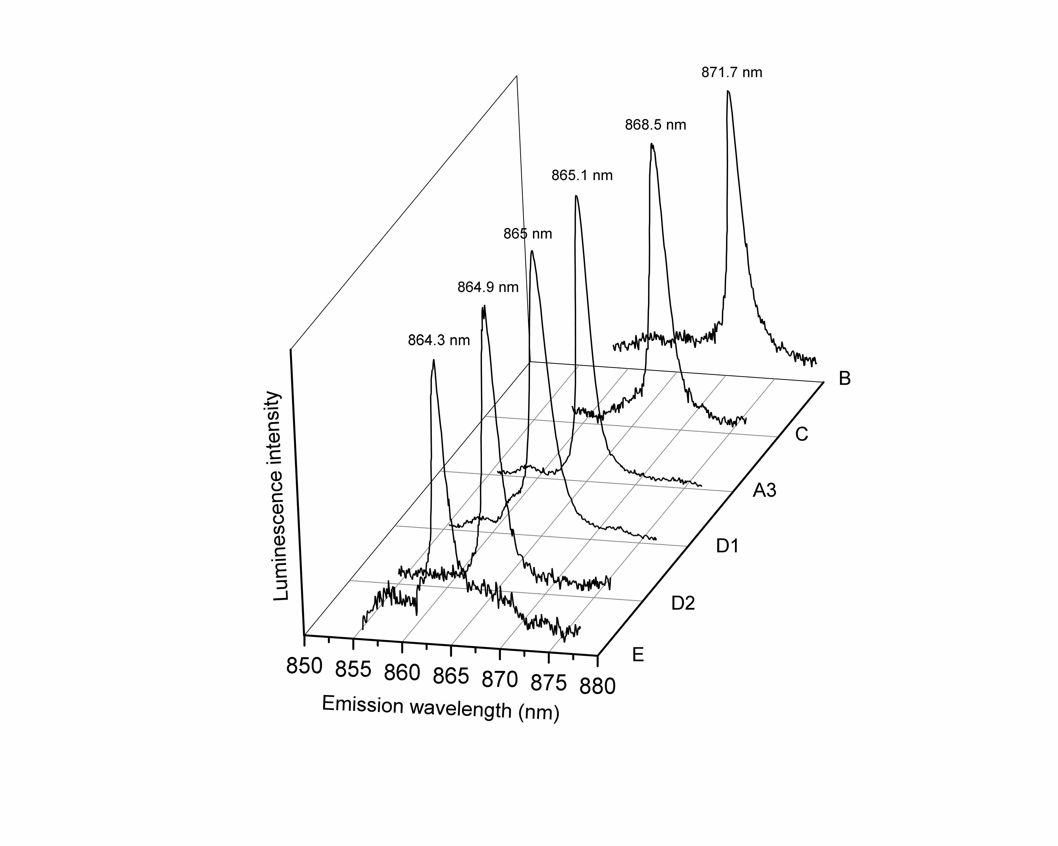
Figure 2. Dependence of the ZPL spectral shape of Ni-Si related complex impurity center in diamond nanograins on deposition conditions. The spectra were recorded by 488 nm laser excitation at room temperature.
Preparation of nanocrystalline diamond and nanocrystalline silicon carbide by ultrashort laser pulses
Favorable properties of color centers formed in nanodiamond for various applications in quantum informatics, medical imaging and biolabeling generate a need to develop fast, reliable and widespread technology for their fabrication. Therefore a new concept was introduced for the creation of one-photon emitter centers in nanodiamond by using ultrashort laser pulses (800 nm center wavelength with 1 kHz repetition rate and 42 fs pulse duration). Nanodiamond crystals were produced with ultrashort laser pulses by using different carbon- and silicon-based materials as source material. Surface-enhanced Raman spectroscopy measurements were performed to prove the presence of diamond nanocrystals (Fig. 3, left). The incorporation of silicon foreign atoms into the nanodiamond structure under laser irradiation was also demonstrated.
|
|
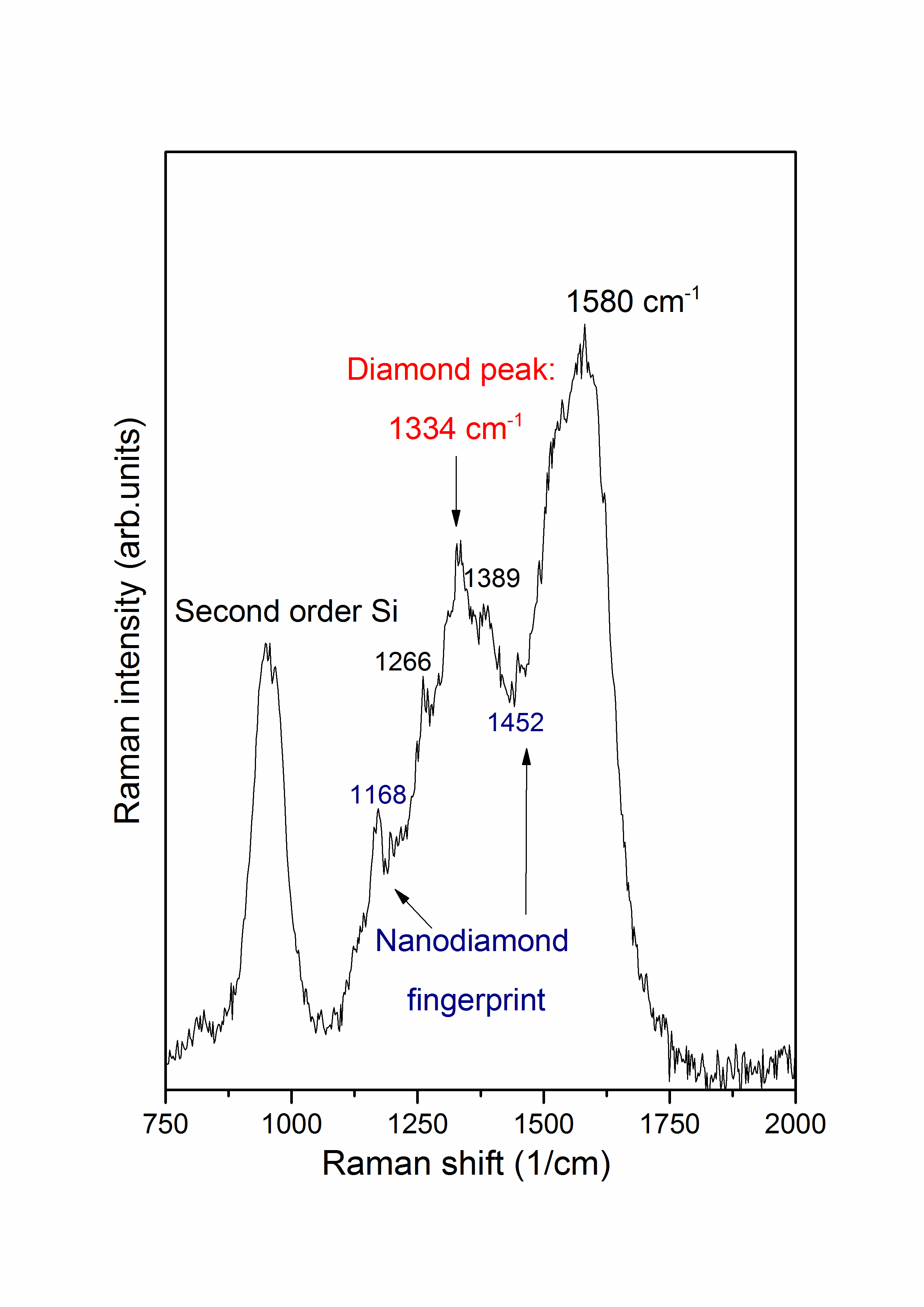
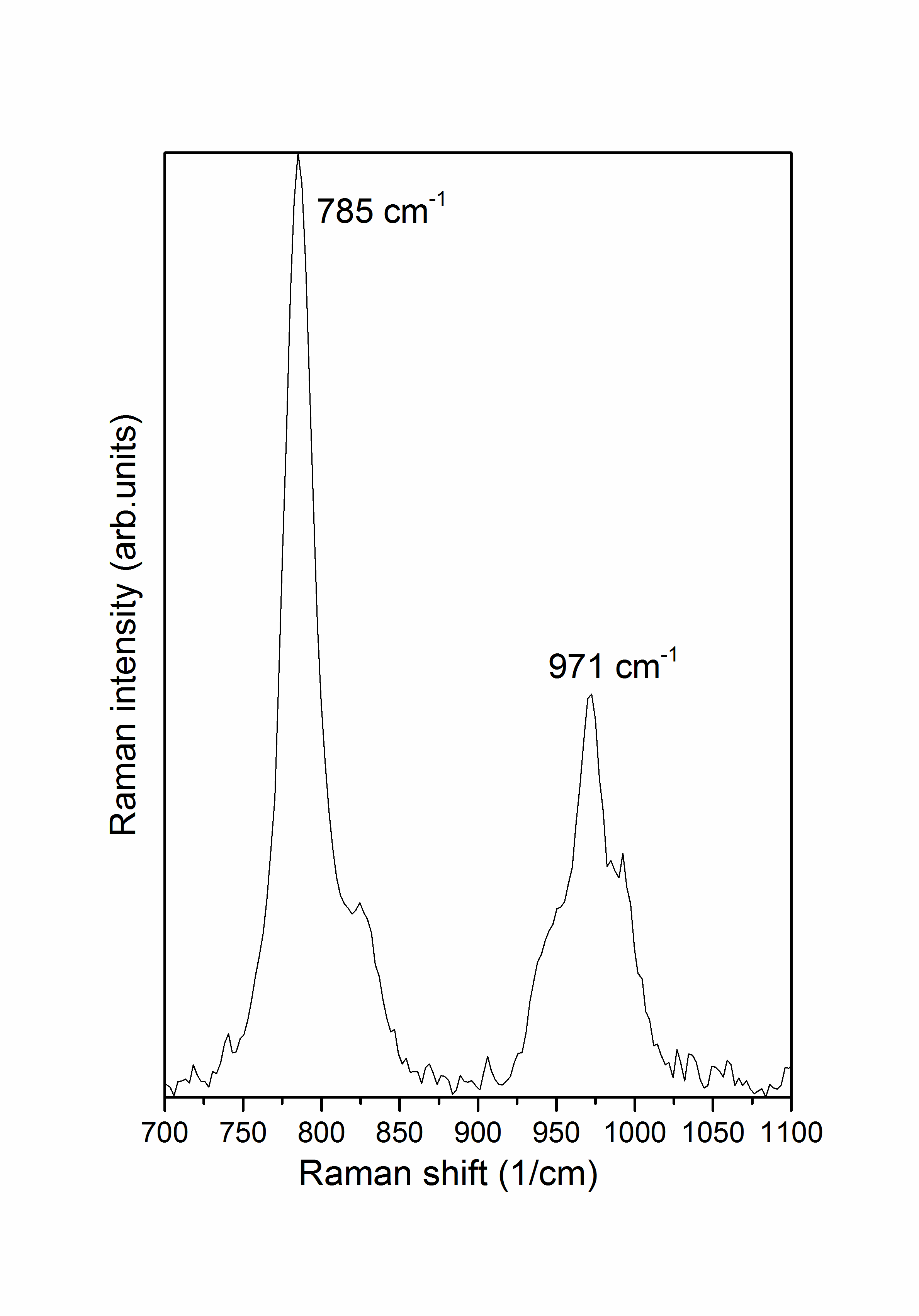
Figure 3.(Upper) Surface-enhanced Raman scattering spectrum of nanocrystalline diamond grains. (Down) Micro-Raman spectrum of the silicon carbide agglomerate excited by 514 nm probing wavelength.
Silicon carbide (SiC) nanocrystals were created successfully by the irradiation of carbon- and silicon-based materials with femtosecond laser pulses (800 nm center wavelength with 1 kHz repetition rate and 42 fs pulse duration) in air at room temperature. Micro-Raman spectroscopic and scanning electron microscopy measurements were carried out to prove the presence of SiC nanocrystals and to analyze the bonding structure of formed nanostructures. Detailed analysis of the transversal (TO) and longitudinal (LO) optical modes support the formation of cubic and hexagonal SiC nanocrystals (3C, 4H and 6H) with average grain size of 100-500 nm (Fig. 3, right).
Kapcsolat
Phone center: +36-1-392-2222
Secretary of the Director General: +36-1-392- 2512
E-mail: wigner@wigner.hun-ren.hu
Media contact: +36-30-487-9869